Monolithic diodes And Monolithic Capacitors
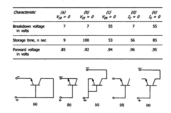
Table of Contents
Monolithic Diodes, Monolithic Capacitors, Integrated Resistors, Diffused Resistor
Diode, an Electrical Component that allows the flow of current in only one direction
Monolithic Diodes
Using Transistor structures in one of the five possible connections, Integrated circuit diodes are created. Figure displays the three most common structures. One of the following structures is used to create the diode from a Transistor structure.
1. The Emitter-base diode, with Collector short Circuited to the base.
2. The Emitter-base diode with the Collector open
3. The Collector –base diode, with the emitter Open-circuited.
The desired performance and application determine the diode structure to be used. Collector-base diodes are appropriate for Common-cathode diode arrays Diffused within a single Isolation island because they have higher Collector-base arrays breaking ratings. When the Reverse-voltage Requirement of the circuit does not exceed the lower Base-emitter Breakdown voltage, the Emitter-base Diffusion is a very common method for making diodes.
Monolithic Diodes
Integrated Resistors
Utilizing the Diffused volume of Semiconductor Region’s bulk Resistivity, a Resistor is created in a Monolithic Integrated circuit. The following techniques are Frequently used to create Integrated Resistors: 1. Diffused 2. Epitaxial 4. Thin film techniques, including pinched.
Diffused Resistor
During base or emitter Diffusion Processes, the Diffused Resistor can form in any one of the Isolated regions of the Epitaxial layer. Due to the parallel production of this type of Resistor and bi-polar Transistor, it is very Cost-effective. The Monolithic Resistor is Typically realised using the N-type emitter Diffusion and P-type base Diffusion.
The Diffused Resistor has a serious Drawback in that it can only be produced in small valued Resistors. The resistance value is determined by the surface Geometry, including the length, width, and Diffused Impurity profile. The sheet resistance is a term used to describe this resistance that is Frequently used. It is described as the resistance provided by the Diffused area, Measured in Ohms/square.
In the Monolithic Resistor, the resistance value is Expressed by R = Rs 1/w
where R= resistance offered (in ohms)
Rs = sheet resistance of the particular Fabrication process involved (in Ohms/square)
l = length of the Diffused area and w = width of the Diffused area.
The base and Emitter’s sheet resistances are 200/Square and 2.2/Square, respectively. For instance, a strip with an emitter will have a resistance of 22 if it is 2 mil wide and 20 mil long. The diffusion region can be formed in a zigzag pattern, producing a longer effective length, for higher resistance values. The realisation of resistors is another application for the poly silicon layer.
Epitaxial Resistor
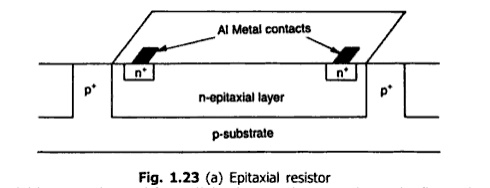
The N-epitaxial layer can be used for realizing large resistance values. The figure shows the cross-sectional view of the epitaxial resistor formed in the epitaxial layer between the two N+aluminium metal contacts.
Pinched resistor
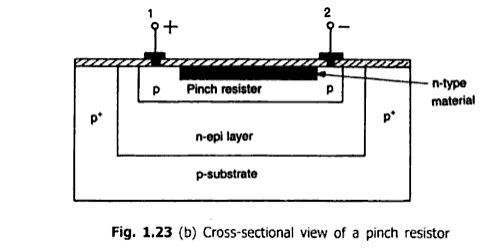
By reducing the cross-sectional area of the diffusion regions, the sheet resistance they provide can be raised. In the base region, this kind of resistance is typically attained. Figure depicts a diffused resistor with a pinched base. It can provide mega ohm-order resistance in a comparatively smaller space. Since the diode realised at contact 2 is biassed in the opposite direction, no current can flow in the N-type material in the structure depicted. Because the current has been decreased or pinched, only a very small amount of reverse saturation current can flow in the conduction path. As a result, as the width decreases, the resistance between contacts 1 and 2 rises, acting as a pinched resistor.
Thin film resistor
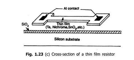
Monolithic resistors can also be made using the thin film deposition technique. Vapour deposition methods are used to deposit a very thin metallic film on the silicon dioxide layer, with a thickness of less than 1 m. Nichrome (NiCr) is typically employed in this process. To obtain the desired geometry and the right value of resistors, masked etching processes are used. Aluminum metallization, which was covered in earlier sections, is used to create ohmic contacts.
The cross-sectional view of a thin film resistor as shown in figure. Sheet resistances of 40 to 400Ω/ square can be easily obtained in this method and thus 20kΩ to 50kΩ values are very practical.
The advantages of thin film resistors are as follows:
1. They have smaller parasitic components which makes their high frequency behaviour good.
2. The thin film resistor values can be very minutely controlled using laser trimming.
3. They have low temperature coefficient of resistance and this makes them more stable.
The thin film resistor can be obtained by the use of tantalum deposited over silicon dioxide layer. The main disadvantage of thin film resistor is that its fabrication requires additional processing steps.
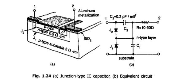
Monolithic Capacitors
Since they have a narrow range of values that can be obtained and poor performance, monolithic capacitors are not frequently used in integrated circuits. The collector-base or emitter-base diffusion of the transistor forms a reverse biassed PN junction, of which there are two types: junction capacitors. The capacitance is inversely proportional to the depletion thickness and proportional to the junction area.
C α A, where a is the area of the junction and
C α T , where t is the thickness of the depletion layer.
The capacitance value thus obtainable can be around 1.2nF/mm2 .
The thin film or metal oxide silicon capacitor uses a thin layer of silicon dioxide as the dielectric. One plate is the connecting metal and the other is a heavily doped layer of silicon, which is formed during the emitter diffusion. This capacitor has a lower leakage current and is Non-directional, since emitter plate can be biased positively. The capacitance value of this method can be varied between 0.3 and 0.8nF/mm2 .
Inductors:
There are no Reliable Integrated Inductors available. A wound Inductor that is connected Externally to the chip Typically supplies high Q Inductors with Inductance values greater than 5 H. As a result, when using Integrated Circuits, Inductors are Typically avoided. (Monolithic Diodes)
Monolithic Diodes
Constant current source
Current Mirror
A constant current source makes use of the fact that for a transistor in the active mode of operation, the collector current is relatively independent of the collector voltage. In the basic circuit shown in fig 1
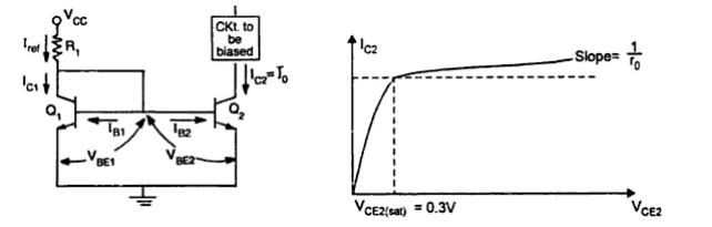
Transistors Q1&Q2 are matched as the circuit is fabricated using IC technology. Base and emitter of Q1&Q2 are tied together and thus have the same VBE. .In addition, transistor Q1 is connected as a diode by shorting it s collector to base. The input current Iref flows through the diode connected transistor Q1 and thus establishes a voltage across Q1.
This voltage in turn appears between the base and emitter of Q2 .Since Q2 is identical to Q1, the emitter current of Q2 will be equal to emitter current of Q1 which is approximately equal to Iref
As long as Q2 is maintained in the active region ,its collector current IC2=Io will be approximately equal to Iref .
Since the output current Io is a reflection or mirror of the reference current Iref, the circuit is often referred to as a current mirror.
Analysis:
The collector current IC1 and IC2 for the transistor Q1 and Q2 can be approximately expressed as
From equations b>>1, b/(b+2) is almost unity and the output current I0 is equal to the reference current, Iref which for a given R1 is constant. Typically Io varies by about 3% for 50 ≤ b ≤200.
It is possible to obtain current transfer ratio other than unity simple by controlling the area of the emitter-base junction (EBJ) of the transistor Q2 . For example, if the area of EBJ of Q2 is 4 times that of Q1,then
IO=4 Iref
The output resistance of the current source is the output resistance,r0 of Q2,
The circuit however operates as a constant current source as long as Q2 remains in the active region.