Differential Amplifier
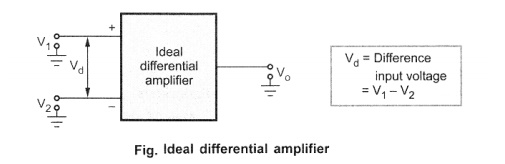
Table of Contents
Differential Amplifier
Introduction of Differential Amplifier
An Amplifier is a device that accepts an input signal and outputs a signal that is Proportional to the input. Differential Amplifiers are those that boost the differences between the two input signals. Different Analogue Circuits use the Differential Amplifier Configuration. A Fundamental and important Component of Contemporary Integrated circuit Amplifiers is the Differential Amplifier. Nowadays, complex circuit design has become incredibly simple thanks to the Widespread use of Integrated circuit (IC) technology. The Operational Amplifier in Integrated circuit (IC) form is less expensive, smaller, and uses less energy. The fundamental component of such an IC Operational Amplifier is the Differential Amplifier.
Basics of Differential Amplifier
The Differential Amplifier Amplifies the difference between two input voltage signal. Hence it is also called as difference Amplifier.
Consider an ideal Differential Amplifier shown in the Fig. A
V1 and V2 are the two input signals while Vo is the output. Each signal is Measured with respect to the ground.
In an ideal Differential Amplifier, the output voltage Vo is Proportional to the difference between the two input signals. Hence we can write,
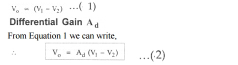
where AD is the constant of Proportionality. The AD is the gain with which Differential Amplifier Amplifies the difference between two input signals. Thus it is called Differential gain of the Differential Amplifier.
Thus, Ad = Differential gain
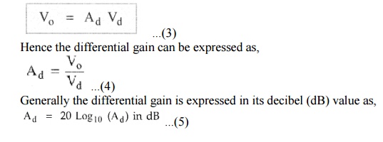
The difference between the two inputs (V1 – V2) is generally called difference voltage and denoted as Vd.
Common Mode Gain Ac
The output voltage Vo = (V1 – V2) Ad should ideally be zero if two identical input voltages, V1 = Vz, are applied to the differential amplifier. However, the practical differential amplifier’s output voltage also depends on the average common level of the two inputs in addition to the difference voltage.
Such an average level of the two input signals is called common mode signal denoted as VC
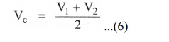
Practically, the differential amplifier produces the output voltage proportional to such common mode signal, also.
The gain with which it amplifies the common mode signal to produce the output is called common mode gain of the differential amplifier AC.

Thus there exists some finite output for V1 = V2 due to such common mode gain AC, in case of practical differential amplifiers.
So the total output of any differential amplifier can be expressed as,

For an ideal differential amplifier, the differential gain Ad, must be infinite while the common mode gain must be zero.
But due to mismatch in the internal circuitry, there is some output available for
V1 = V2 and gain AC is not practically zero. The value of such common mode gain AC very small while the value of the differential gain Ad is always very large.
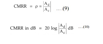
Common Mode Rejection Ratio (CMRR)
The differential amplifier is said to be operating in common mode when the same voltage is applied to both inputs. Numerous interference and noise signals show up at both input terminals of the differential amplifier as a common input signal. The differential amplifier should reject such a common signal. A ratio known as the common mode rejection ratio, abbreviated as CMRR, describes an amplifier’s capacity to reject a common mode signal.
It is defined as the ratio of the differential voltage gain Ad to common mode voltage gain AC
Transistorised Differential Amplifier
The transistorised differential amplifier basically uses the emitter biased circuits which are identical in characteristics. Such two identical emitter biased circuits are
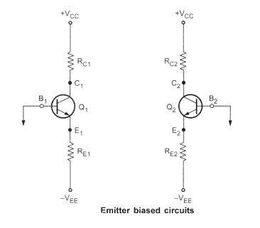
And The two transistors Q1 and Q2 have exactly matched characteristics. The two collector Resistors R C1 and R C2 are equal while the two emitter resistances R E1 and R E2 are equal.
RC1 = RC2
And
RE1 = RE2
The magnitudes of + Vcc and – V EE are also same. The differential amplifier can be obtained by using such two emitter biased circuits. This is achieved by connectinemitter E1 of Q1 to the emitter E2 of Q2. Due to this, R E1 appears in parallel with R E2and the combination can be replaced by a single resistance denoted as R E. The base B1of Q1 is connected to the input 1 which is V S1 while the base B 2 of Q2 is connected tothe input 2 which is Vs2. The supply voltages are measured with respect to ground. Thebalanced output is taken between the collector C1 of Q1 and the collector C2 of Q 2. Suchan amplifier is called emitter coupled differential amplifier. The two collectorresistances are same hence can be denoted as R C..
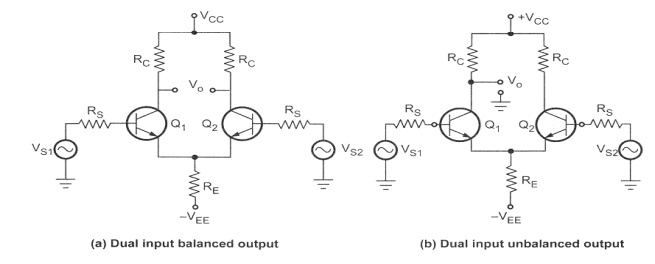
Alternatively, the output can be placed between one of the two collectors and the ground. It is known as balanced output, double ended output, or floating output when the output is divided between the two collectors and neither of them is grounded. Unbalanced output or single ended output refers to the output that is taken between any of the collectors and the ground. A basic dual input, balanced output differential amplifier’s entire circuit diagram is depicted in Fig.
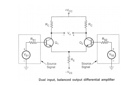
As the output is taken between two output terminals, none of them is grounded, it is called balanced output differential amplifier.
Let us study the circuit operation in the two modes namely
i) Differential mode operation
ii) Common mode operation
Differential Mode Operation
The two input signals differ from one another in differential mode. Take into account the two input signals, which share the same magnitude but are 180° out of phase. The centre tap transformer can produce these opposite-phase signals. The circuit used in differential mode operation is shown in the Fig..
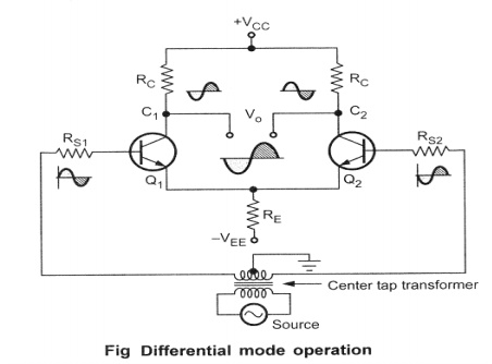
Assume that the sine wave on the base of Q 1is positive going while on the base of Q 2 is negative going. With a positive going signal on the base of Q 1, m amplified negative going signal develops on the collector of Q1. Due to positive going signal, current through R E also increases and hence a positive going wave is developed across R E. Due to negative going signal on the base of Q2, an amplified positive going signal develops on the collector of Q 2.
And a negative going signal develops across R E, because of emitter follower action of Q 2. So signal voltages across R E, due to the effect of Q1 and Q2 are equal in magnitude and 180o out of phase, due to matched pair of transistors. Hence these two signals cancel each other and there is no signal across the emitter resistance. And Hence there is no a.c. signal current flowing through the emitter resistance.
Hence R E in this case does not introduce negative feedback. While Vo is the output taken across collector of Q1 and collector of Q 2. The two outputs on collector L and 2 are equal in magnitude but opposite in polarity. And Vo is the difference between these two signals, e.g. +10 – (-10) = + 20.
Hence the difference output Vo is twice as large as the signal voltage from either collector to ground
common Mode operation
The signals applied to Q1 and Q2’s bases in this mode come from the same source. The two signals are therefore equal in both magnitude and phase. The circuit diagram is shown in the Fig.
In phase signal voltages appear across R E and combine with in phase signal voltages at the bases of Q1 and Q2. As a result, R E produces negative feedback and carries a signal current. The differential amplifier’s common mode gain is decreased by this feedback.
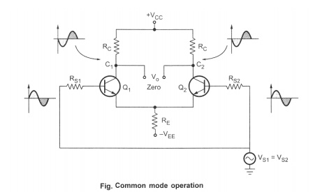
While the two signals causes in phase signal voltages of equal magnitude to appear across the two collectors of Q 1 and Q2. Now the output voltage is the difference between the two collector voltages, which are equal and also same in phase,
Eg. (20) – (20) = 0. Thus the difference output Vo is almost zero, negligibly small. ideally it should be zero.
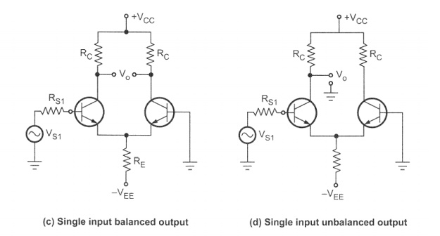
Configurations of Differential Amplifier
The Differential Amplifier, in the difference Amplifier stage in the op-amp, can be used in four Configurations :
i) Dual input Balanced output Differential Amplifier.
ii) Dual input, Unbalanced output Differential Amplifier.
iii) Single input, Balanced output differential amplifier.
iv) Single input, Unbalanced output differential amplifier.
The Differential Amplifier uses two transistors in common emitter configuration. If output is taken between the two collectors it is called balanced output or double ended output. While if the output is taken between one collector with respect to ground it is called unbalanced output or single ended output. If the signal is given to both the input terminals it is called dual input, while if the signal is given to only one input terminal and other terminal is grounded it is called single input or single ended input Out of these four configurations the dual input, balanced output is the basic differential amplifier configuration.
This is shown in the Fig. (a). The dual input, unbalanced output differential amplifier is shown in the Fig.(b). The single input, balanced output differential amplifier is shown in the Fig (c) and the single input, unbalanced output differential amplifier is shown in the Fig. (d).
D.C. Analysis of Differential Amplifier
The d.c. analysis allows for obtaining the I Cq and V CEQ operating point values for the transistors used. Since the input signals are a.c. while the supply voltages are d.c., it is easy to create a d.c. equivalent circuit by simply reducing the input a.c. signals to zero. The resulting d.c. equivalent circuit is depicted in Fig. The source resistance is simply represented by Rs if Rs1 = R s2.
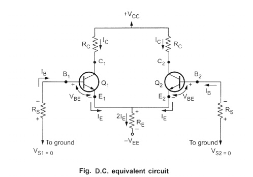
The Transistors Q1 and Q 2 are matched Transistors and hence for such a matched pair we can assume :
i) Both the Transistors have the same Characteristics.
ii) R E1 = R E2 hence R E= R E1 ll R E2.
iii) R C1 = R c 2 hence denoted as R C.
iv) lV CCI = lV EE I and both are Measured with respect to ground.
As the two Transistors are matched and circuit is Symmetrical, it is enough to find out
operating point I CQ and V CEQ, for any one of the two Transistors. The same is Applicable for the other Transistor.
Apply-g KVL to Base-emitter loop of the Transistor Q1,