Transistor: Types, Construction, Currents
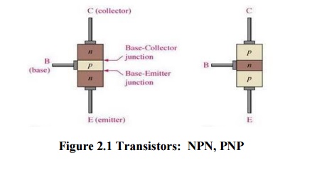
Table of Contents
TRANSISTOR, TRANSISTOR TYPES, Forward bias, Reverse bias
TRANSISTOR Basics
The Transistor is the primary “element” or building block of electronics. It is a Semiconductor device, and there are two main types of it: field effect Transistors (FETs) and Bi-polar Junction Transistors (BJTs) (FET).
The word “Transistor,” which is an acronym for “Transfer-of-resistor,” is used to describe it. It means that Depending on the Biassing voltage applied to the Transistor, the internal resistance of the Transistor changes from one value to another. Hence, it is also known as a transfer Resistor.
TRANSISTOR
The operation of a three Terminal Semiconductor device known as a Bi-polar Transistor (BJT) depends on the Interaction of both Majority and Minority Carriers, thus the name “Bi-polar.”
The third Terminal’s current is controlled by the voltage between two other Terminals. Therefore, it is known as a current controlled device. This is the BJT’s fundamental tenet.
It can be used as Amplifier and logic Switches. BJT Consists of three Terminals:
Collector : C
Base : B
Emitter : E
TRANSISTOR TYPES
Two Varieties of Bi-polar Transistors exist.
- NPN Transistor
- PNP Transistor
1. TRANSISTOR CONSTRUCTION
PNP Transistor: A thin layer of N-type silicon is Positioned between two layers of P-type silicon in a PNP Transistor.
NPN Transistor: A thin layer of P-type silicon is Sandwiched between two layers of N-type silicon in an NPN Transistor.
The two types of BJT are Represented in figure 2.1
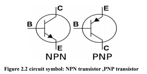
The Symbolic Representation of the two types of the BJT is shown in figure 2.2
Area:[C>E>B]
The collector layer’s area is the largest. so that heat can be quickly dissipated. The base layer is the thinnest and has the smallest area. Medium-sized emitter layer area.
Doping level: [E>C>B]
Collector layer has a medium doping level. Thus, it has a Moderate amount of charges. Lightly doped is the base layer. As a result, there are not many charges. The emitter layer has a lot of doping. Therefore, it has the most charges.
Junctions:
There are two junctions in this transistors – junction J-1 and junction J-2.
The junction between collector layer and base layer is called as collector-base junction or C-B junction.
The junction between base layer and emitter layer is called as base-emitter junction or B-E junction. The two junctions have almost same potential barrier voltage of 0.6V to 0.7V, just like in a diode.
Equivalent diode Representation:
The Transistors formed by Back-to-back connection of two diodes
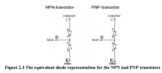
The external circuitry connected to the transistor can change the states of the two pn junctions. The transistor is being biassed in this process.
Usually the emitter- base junction is forward biased and collector –base junction is reverse biased. Due to forward bias on the emitter- base junction an emitter current flows through the base into the collector. Though, the collector –base junction is reverse biased, almost the entire emitter current flows through the collector circuit.
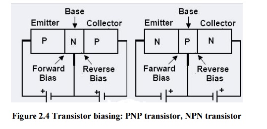
A single pn junction has two different types of bias:
Forward bias
Reverse bias
There are two junctions in Bi-polar junction transistors. Each junction can be forward or reverse biased independently. Thus there are four modes of operations:
Forward Active
Emitter-base junction is forward biassed and collector-base junction is reverse biassed in this mode of operation. The transistor acts like a source. The BJT can be utilised in analogue circuits and as an amplifier by having controlled source characteristics.
Cut off
Cut off mode is used when both junctions are reverse biassed. Since there is essentially no current flowing, the transistor acts like an open switch in this scenario.
Saturation
In saturation mode both junctions are forward biased large collector current flows with a small voltage across collector base junction. Transistor behaves as an closed switch.
Reverse Active
This emitter base junction is reverse biassed and the collector base junction is forward biassed, making it the opposite of the forward active mode. Inverted mode is the name of the mode. It can’t be amplified, sorry. However, digital circuits and some analogue switching circuits can use the reverse active mode.
2. TRANSISTOR CURRENT
The arrow is always drawn on the emitter The arrow always point toward the n-type
The arrow indicates the direction of the emitter current:
pnp: E-> B
npn: B-> E
IC = the collector current, IB = the base current, IE = the emitter current
OPERATION OF AN NPN TRANSISTOR
The collector base junction has a reverse bias, whereas the emitter base junction has a forward bias. Many electrons from the emitter are entering the base region because the emitter base junction is forward biassed. P-type impurity is lightly doped into the base. Therefore, there are very few holes in the base region.
Due to this, electron- hole recombination is less (i.e,) few electrons(<5%) combine with holes to constitute base current(IB)
The remaining electrons (>95%) crossover into collector region, to constitute collector current(IC).
OPERATION OF A PNP TRANSISTOR
The Collector base Junction has a reverse bias, whereas the emitter base Junction has a forward bias. Due to the forward bias of the emitter base Junction, a lot of holes from the emitter enter the base region and Electrons from the base enter the emitter region. N-type Impurities are lightly doped into the base. Therefore, there are very few Electrons in the base region.
As a result, there is less Electron-hole Recombination, i.e., only about 5% of holes combine with Electrons to form base current (IB)