


Mengapa Memilih PLAY288 pada Tahun 2025?
Di tengah banyaknya situs permainan slot online baru setiap hari, PLAY288 hadir sebagai jawaban atas kebutuhan akan pengalaman bermain yang aman, lengkap, dan tentunya BIG WIN untuk para anggota. PLAY288 tidak hanya menyediakan berbagai macam permainan, tetapi juga menjadi situs terpercaya yang banyak digunakan oleh ribuan pemain di Asia.
Mungkin menjadi tantangan bagi pemain pemula dan menengah untuk menemukan situs slot online terbaik. Namun, dengan gaya baru yang hebat dan sistem keamanan teratas, PLAY288 telah mampu menjadi salah satu situs terbaik di tahun 2025.
PLAY288 Sebagai Situs Permainan Slot Online Terpercaya
Apa saja keunggulannya?
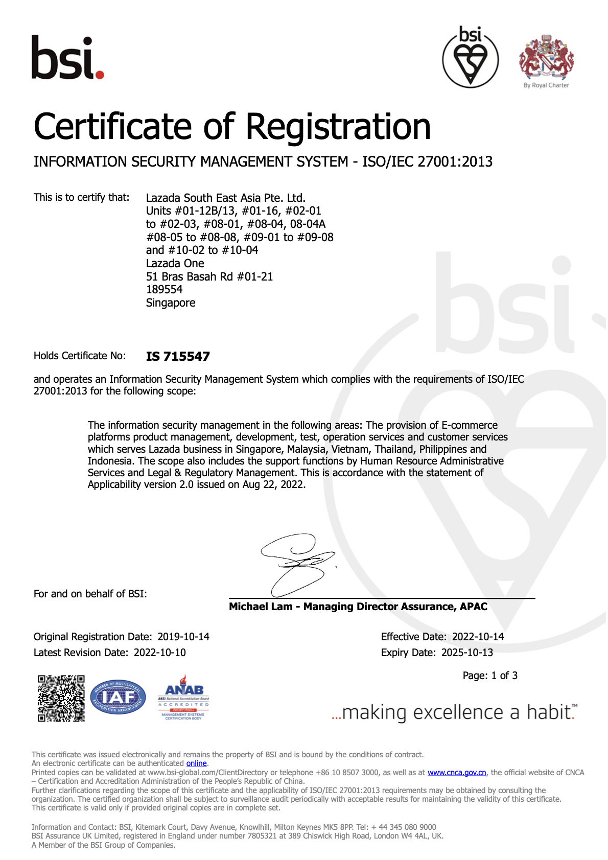
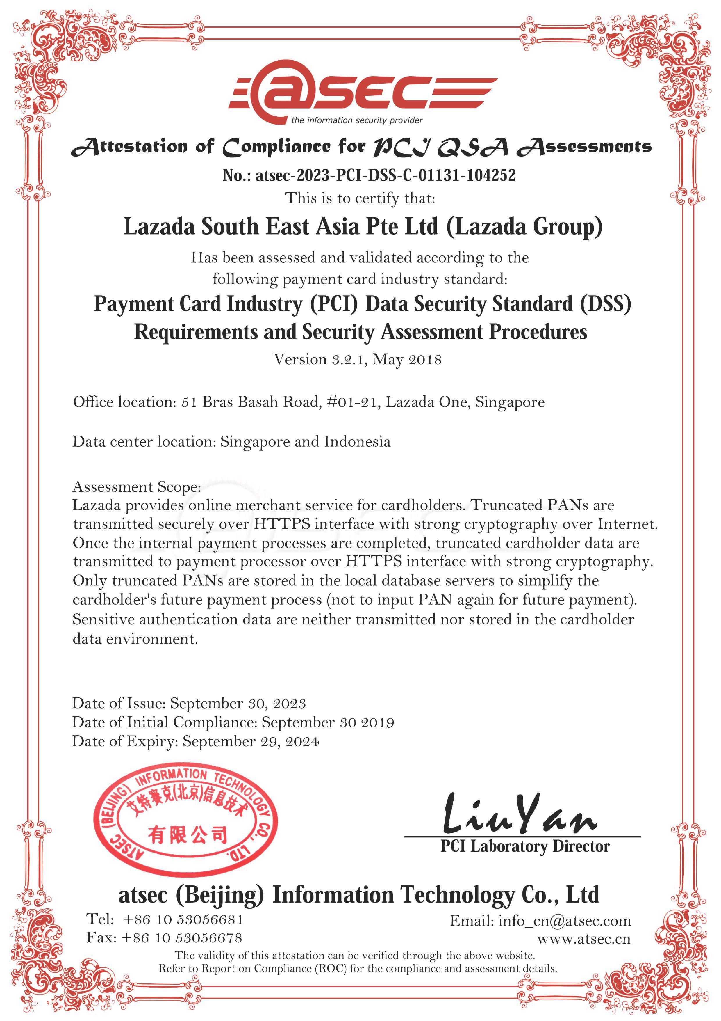
🔐 1. Legal dan AmanPLAY288 bangga menjadi kasino berlisensi dan diatur di pasar internasional dengan asosiasi yang adil tersedia. Ini memastikan setiap transaksi dan permainan bersifat transparan dan aman.
🎮 2. Permainan Slot TerlengkapJenis permainan yang ditawarkan oleh PLAY288 mencapai ribuan dari slot klasik hingga video slot modern terbaru; semua dari penyedia paling dikenal seperti Pragmatic Play, PG Soft, Habanero, dan Microgaming.
⚡ 3. Proses Deposit & Penarikan SupersonikTransaksi hanya dalam hitungan detik! Itu bisa melalui transfer bank, dompet digital, atau QRIS tanpa hambatan.
🎁 4. Bonus Harian MenarikAnda bisa mendapatkan Bonus Harian, Cashback Mingguan, dan Jackpot Mingguan untuk Anda ikuti di situs mereka. Semuanya dibuat agar Anda memiliki lebih banyak cara untuk menang.
📱 5. Dapat Dimainkan di Semua PerangkatMainkan mesin slot di PC, tablet, atau ponsel? Semuanya berjalan lancar. Desain situs web PLAY288 kompatibel dengan semua ukuran layar dan OS.
Tips Bermain Permainan Slot Online untuk Pemain Pemula
Untuk bermain dan bukan hanya bermain, tetapi menang dengan strategi, berikut adalah daftar hal yang dapat Anda lakukan agar tetap bertahan.
✅ Pilih slot dengan RTP (Return to Player) tertinggi (>95%) untuk meningkatkan peluang Anda menang.
✅ Mainlah dengan hadiah pertama tanpa menyetor uang besar.
✅ Tetapkan batas harian seberapa banyak Anda ingin bermain untuk mencegah pengeluaran berlebih.
✅ Mainkan permainan demo terlebih dahulu, terutama dengan permainan baru dan tidak dikenal.
✅ Gunakan fitur auto-spin secara selektif, jangan sampai saldo meledak dalam bagian ketika auto spin dinyalakan.
Pengindeksan Semantik Lateral (LSI) kata kunci
- situs slot resmi 2025
- permainan slot online "gacor" (gacor adalah istilah untuk permainan slot yang baik)
- pendaftaran slot terpercaya
- slot RTP tinggi
- slot link anti blokir
- permainan slot yang nyaman
- slot aman dan mudah menang
Lihat juga Jika Anda tidak dapat menemukan jawaban yang Anda cari, silakan merujuk ke bagian FAQ kami.
- Apakah PLAY288 aman untuk pendatang baru?Ya, sangat aman. Sistem keamanan dan permainan adil PLAY288 menggunakan sistem keamanan standar internasional, semua teknologi mutakhir untuk memastikan keamanan permainan Anda.
- Apakah saya harus menggunakan VPN untuk bermain di PLAY288?Tidak perlu. Link PLAY288 anti blokir dan dapat diakses langsung dari Indonesia tanpa menggunakan perangkat VPN.
- Berapa deposit minimum di PLAY288?Anda dapat bermain dengan hanya deposit Rp10.000.
- Apa saja manfaat dari permainan slot di PLAY288 dibandingkan dengan situs lain?Selain menawarkan berbagai macam permainan, RTP tinggi, dan antarmuka yang ramah pengguna, transaksi cepat dan dukungan 24/7 membuatnya menjadi daya tarik tambahan.


 Promosi
 Login
Login
 Home
Home
 Whatsapp
 Live Chat